FAQ: how are full and semi custom ASICs verified?
20 Nov 2017 by 7400ASIC designs are written in a C-like language called Verilog. This language allows us to verify our designs by simulation. Verification means that we test our designs before building anything physical. This is critical because ASIC tooling costs are in the millions, and one mistake can mean the tooling will spoiled, costing millions and months of schedule delay. And that could be a fatal mistake.
Verification by simulation and FPGA
There are two main levels of logic verification. The first is simulation that runs on a computer, much like VMWare executing a virtual PC. We use a Verilog simulator by Synopsys called VCS, which is really fast as simulators go. However it is really slow compared to the real thing. So we use it during development to test only parts of the chip, or for limited tests of the full chip. These are the so called regression tests.
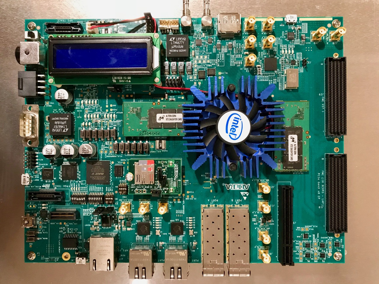
The second level of verification is actually implementation on an FPGA, which is essentially a reprogrammable ASIC. We use a 20nm FPGA system by Altera. It allows us to build an instance of our ASIC at the cost of the thousands of dollars, not millions. Typically an ASIC implemented on the FPGA runs ten times slower than the physical ASIC because clock rate and size are not as great as the real thing.
The big advantage of FPGA implementation is that while it’s not the real thing, it is still powerful enough to enable real time system testing, so called end to end test. It’s like getting chips six months early. Our test system consists of Decred’s reference gominer running on a Raspberry Pi, talking to our ASIC implemented on the FPGA. Thus we have a full dcrASIC mining system.
So today, even before tapeout, we have high confidence in our design because our ASIC has already been mining pool shares. We’ve probably only made pennies on it. But those pennies are worth millions.
2017-11-14 21:44 [INF] MINR: Global stats: Accepted: 90
Integrity of the production ASIC
Now the critical part in this whole process is that the FPGA and production ASIC implementations need to faithfully reproduce the behavior programmed in Verilog. One tiny deviation can be fatal.
The key here is a machine translation process called “synthesis” that is akin to compiling a C program to a binary executable. Like C compilation, synthesis ensures that the resulting FPGA implementation behaves exactly as programmed. The synthesis tool we use is Design Compiler by Synopsys. In the FPGA case, the result is a binary file that is loaded into the FPGA at power-up.
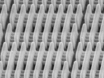
For the production ASIC, the ultimate result of synthesis is a GDSII file. GDSII is essentially the blueprint that the factory uses to mass produce the ASIC; it specifies where to put all the transistors and how to wire them all together. The transistors are organized into “standard cells” that implement primitive functions like a NAND gate or flip flop. The standard cell library contains the blueprints for these primitives, and synthesis targets this library for the production ASIC. In the C analogy, the standard cell library is like the instruction set that the compiler targets.
The standard cell library is critical to ensuring correctness of the ASIC. One error can mean disaster. As a result, standard cell libraries undergo extensive development, verification, and test, and are supplied fully verified and characterized in real silicon vs voltage, temperature, and process variations. Top tier library vendors such as ARM or Synopsys, have invested millions of man-hours over decades in development. These libraries are also well proven in production. Hundreds of billions of dollars of ASICs for your phone, laptop, car, etc have been built with them.
All this is sound engineering, but still not sufficient to ensure success. The ASIC design process also has many checks to ensure nothing slips through the cracks. We also employ “formal verification” tools that double and triple check everything. These tools examine the various intermediate representations like RTL, netlists, and GDSII, to help ensure integrity. Actually in the C analogy, there is really no comparable step.
Challenges in verifying full custom
But how does this work in full custom? Not as well. The main differences between full and semi custom are: a) that translation is performed by humans instead of machine, and b) that there is no standard cell library, rather primitives like NAND gates are individually designed by hand. The full custom designer is chasing the possibility to better optimize the low level circuitry. (More on the misguided optimizations in a subsequent post.) For this chase, the full custom designer accepts significant compromises to verification and integrity of the ASIC design.
Full custom bypasses synthesis and inserts humans to translate the desired behavior to transistors and physical layout. This is akin to programming a computer in binary op codes. It’s a laborious and error prone process. To understand its complexity, consider that in full custom design something as simple as changing a comparison from LT to LE requires one man week of design time. With all that manual work, errors are introduced. The virtue of full custom has become a liability.
Full custom also requires a third level of simulation – analog simulation. The reason again is because of one of its virtues. Full custom design does not employ the standard cell library. Instead, transistor and physical layout are custom designed for each circuit in the ASIC. Indeed the foundations of the full custom design are weak compared to the fully developed and characterized semi-custom standard cell library.
Thus in full custom even the basic assertion that logic levels are always either one or zero can be violated, in which case the computation is pure nonsense. Further characterization of the circuits is not possible until the first silicon is returned from the fab. Analog simulations are employed to try to mitigate these problems. But those are not a full substitute for characterization of real silicon. And those simulations are orders of magnitude slower than even Verilog simulation. In practice it’s very difficult to simulate even part of a chip. And so the full chip behavior and characteristics are not thoroughly verified and tested, and more bugs creep in.
Finally because full custom employs human transistor design and physical layout, FPGA system testing cannot be used to thoroughly prove the correctness of a full custom chip prior to production.
But wait, don’t the biggest semiconductor companies like Intel employ full custom? Yes they do with teams of thousands of engineers working on it. And their designs have gone through hundreds of iterations to sort out the bugs. They also have multiple tape-outs to characterize silicon before final production. Full custom is a great choice their business. It may not work so well for lower budgets.
The bottom line is that full custom verification is an error prone proposition compared to semi-custom. And so the greater risk of a fatal bug.
Optimizing for success
Success in ASIC design comes from making wise risk tradeoffs. Compound too many risks, and your chances for success become infinitesimal.
It is worth understanding that Bitmain, the big winner in the bitcoin ASIC wars, optimized three generations of their semi-custom design before applying full custom to further optimize their 4th generation. They played the game wisely and won. We agree with this approach, and we are using semi-custom for the first dcrASIC iteration.
Actually there is one other equally important reason why semi-custom is more favorable than full custom, and that is for better optimization, and so better power and performance. That topic will be covered in a subsequent post.
more...